

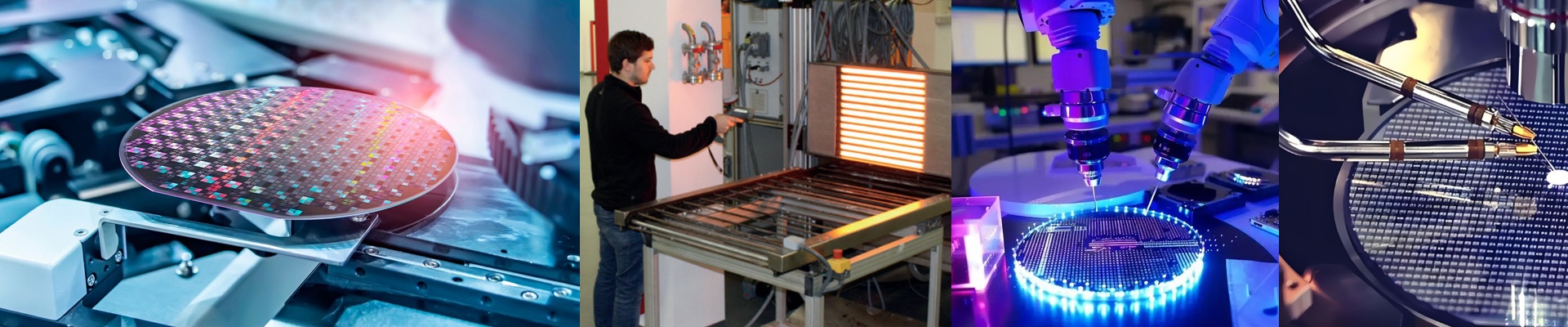

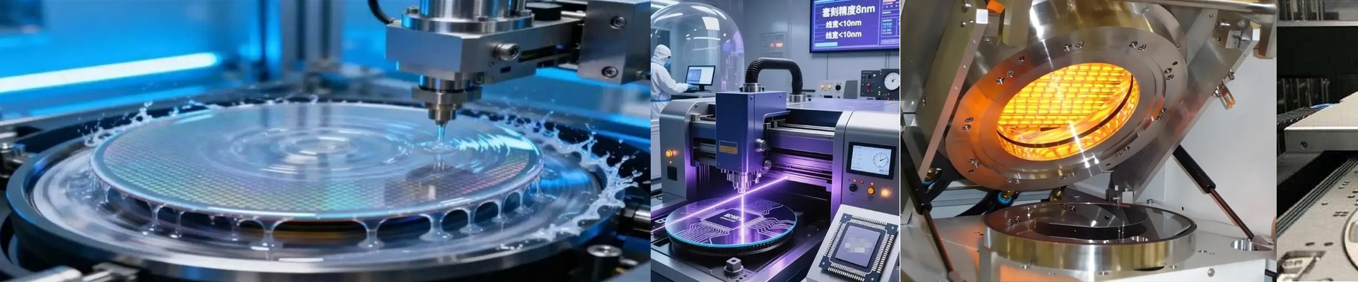
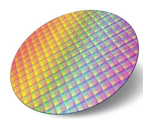
In the fab, drying isn’t just another box to check. It’s the last thermal move before you lock in yield, and it sets the line-of-sight for what comes next. When the hot zone drifts or the energy profile isn’t controlled, you know it immediately—edge bead shows up, solvent hangs around in the track, and the photoresist skin fights you during hard bake. The bill for that comes in rework, scrap, and the quiet cost of wasted energy. What actually matters, technically We run the drying energy audit around infrared heating that’s built for semiconductor work, not for show. The heat lands with sub-millimeter uniformity across the wafer plane, which keeps the temperature distribution repeatable through soft bake and hard bake. That repeatability is what keeps lithography overlay and critical dimension control in the window. The system is cleanroom-compatible from Class 1 to Class 100 and generates zero particles, so particle counts stay where they need to be—on the wafer. Here’s why this lands in a fab: drying performance hits the thermal budget and the bottom line at the same time. The audit pins down the energy draw, flags hot spots, and maps duty cycles so you can cut waste without touching the process. You keep the same throughput, but with fewer kWh, fewer temperature excursions, and less unplanned downtime. The outcome is steady drying across shifts, consistent photoresist bake results, and wafer drying you can count on—again and again. Things to keep in mind when you match infrared delivery to the tool footprint: chamber geometry, the wafer stage, and the existing exhaust path all matter. You also need clean power and solid thermal isolation so uniformity holds up under 24/7 operation. Plan for a tight integration window during preventive maintenance. The payoff is a drying profile you can audit and trust, staying in spec shift after shift.