
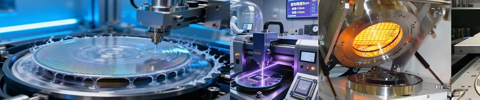
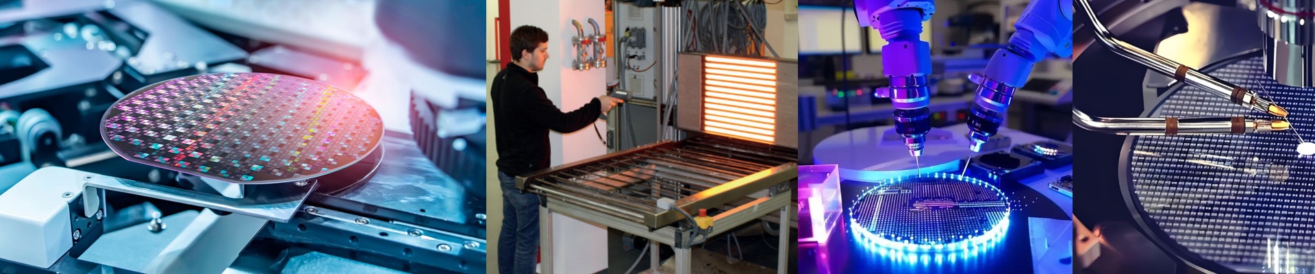
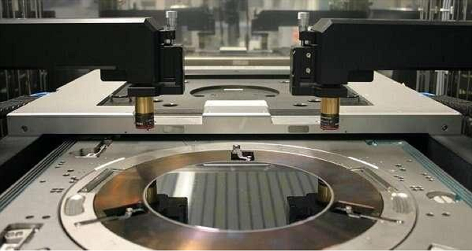
On the fab floor, the clock runs nonstop. Lithography sets the pace, and the bake step right after exposure is where yield either holds steady or starts slipping. Photoresist needs consistent thermal energy—Soft Bake to drive out solvent and lock in dimensions, Hard Bake to set the mask before it hits the etch. Throw the bake off by even a hair, and you watch critical dimension control drift, scum show up after development, and etch selectivity fall apart. You don’t need more heat. You need repeatable heat, delivered where the process needs it, without adding particles or variability. So we built a certified infrared curing lamp line for semiconductor wafer fabrication. It’s engineered around how photoresist actually behaves thermally on wafers, and it’s built to live in Class 1–100 cleanrooms without making life harder.
What matters, technically
We use near-infrared (NIR) emitters with a spectral output shaped to match photoresist absorption. The goal is rapid, volumetric heating without overshooting the substrate. You get a thermal response that’s fast enough for high-throughput lots, but stable enough for sub-degree control. Wafer-level thermal uniformity is held to ±0.1°C across the illuminated zone, measured on standard production wafers with calibrated thermocouples and backed by thermal mapping. That tight band directly supports CD uniformity and cuts down edge-of-field excursions that often trace back to temperature gradients during the bake. Temperature repeatability is specified to ±0.5°C from batch to batch, with closed-loop control and a certified calibration method traceable to recognized standards. For Soft Bake, that repeatability keeps solvent evaporation profiles consistent. For Hard Bake, it preserves the photoresist flow and adhesion the exposure and development steps worked to set. The system is designed to generate zero particle events in operation. The emitter array, reflector geometry, and airflow path are laid out to minimize particulate shedding, and the lamp housing uses materials selected for low outgassing. In practice, that means fewer bake-induced contamination defects—and less time spent on preventive cleaning. Cleanroom compatibility is a requirement, not a tagline. The lamp platform meets Class 1–100 cleanroom demands, with construction that supports ISO Class 3–5 environments and fits into standard fab tool footprints. Reliability comes down to uptime. The emitter module is rated for 24/7 operation, with a service life that supports long campaigns without forcing planned replacement windows. We’ve got units running 5,000+ hours with less than 5% output drop, holding the same temperature setpoints the recipe calls for.
Why it works in real processes
Photoresist processing is a thermal budget problem. Soft Bake has to remove solvent without building in stress that will distort patterns later. Hard Bake has to harden the mask without driving flow that blurs fine features. In both cases, the temperature profile across the wafer matters as much as the setpoint. Our infrared curing lamps deliver that profile with speed and precision. NIR energy penetrates the photoresist layer and heats it volumetrically, so the surface and the bulk don’t fight each other. That reduces the thermal lag that often forces long ramp-up times on hotplates, and it shortens the bake step without sacrificing uniformity. The payoff shows up in the data. When bake temperature is held within ±0.1°C across the wafer and repeatable within ±0.5°C run-to-run, the lithography window tightens. CD control improves. Film thickness after bake becomes more predictable. Etch selectivity behaves the way the models expect, because the photoresist chemistry cures the same way every time. That matters when you run mixed product lots. One recipe may call for Soft Bake at 90°C, another at 110°C, and a third needs Hard Bake at 120°C. The lamp platform hits each setpoint with the same repeatability, so qualification runs don’t need constant retuning when the product mix shifts. Throughput benefits too. Shorter bake cycles cut lot cycle time without compromising quality. That can free up capacity on the lithography track and reduce work-in-progress, especially at nodes where thermal steps start to bottleneck the line. Energy use comes down as well. Infrared heating puts the energy where it’s needed—on the photoresist—instead of heating the whole chuck and surrounding hardware. That reduces thermal load on the tool and the facility, and it lowers the cost per wafer for the bake step.
What you need to keep in mind
Infrared curing is sensitive to line-of-sight and emissivity. Wafer backside metallization, the film stack, and substrate material can all change how the wafer couples thermally to the lamp. That means the lamp configuration—emitter power density, zone mapping, and dwell time—needs tuning to the product stack. We provide a qualification procedure that maps temperature on representative wafers, establishes the recipe, and documents the thermal signature for each product. Installation is straightforward, but the details matter. The lamp integrates into existing lithography tracks through standard mechanical and electrical interfaces, and it needs clean, dry air for cooling plus proper exhaust routing to keep thermal stability. The footprint is compact, but you have to preserve clearances around the illumination zone to avoid stray reflections and protect operators. One constraint is real: infrared curing is optimized for thin films and photoresist layers. If your process needs serious thermal mass—like thick dielectric curing outside the photoresist bake window—a hotplate may still be the better call. For wafer-level Soft Bake and Hard Bake, infrared delivers speed and uniformity with tight control. If you’re qualifying a new node, ramping yield, or trying to tighten CD uniformity, the bake step is a lever you can pull. Our certified infrared curing lamps give you that lever, with thermal precision that matches what modern lithography and etch demand. We’re not selling heat. We’re selling repeatability—measured in degrees, in hours, and in defects avoided.